 FabProcisions
Reverse Engineering Services
Specialized in metrology, mechanical design, machining, and assembly. We reverse-engineer critical semiconductor components to exact specifications.
Precision Engineering & Manufacturing for Semiconductor Equipment
FabProcisions specializes in customized engineering and manufacturing for semiconductor equipment, offering expertise in metrology, 3D scanning, prototyping, and onsite support to meet SEMI industry standards.

Customized engineering and manufacturing services for semiconductor equipment industries in the USA.
Specialized in metrology, mechanical design, machining, and assembly. We reverse-engineer critical semiconductor components to exact specifications.
Site survey, onsite cut/bend/orbital-welding, hookup, and field support. Our team ensures seamless equipment integration in your fab environment.
Expert mechanical design services for custom semiconductor equipment components, from concept through detailed engineering drawings and prototypes.
Precision metrology and 3D scanning for critical semiconductor components and equipment. Form, fit, and function verification at the highest tolerances.
Comprehensive testing and installation services for semiconductor equipment with experienced field support and commissioning.
Skilled assembly and installation services for semiconductor equipment. Precision assembly ensuring optimal performance and reliability.
Precision-engineered heating systems, showerheads, chamber components, and gas systems for semiconductor manufacturing.
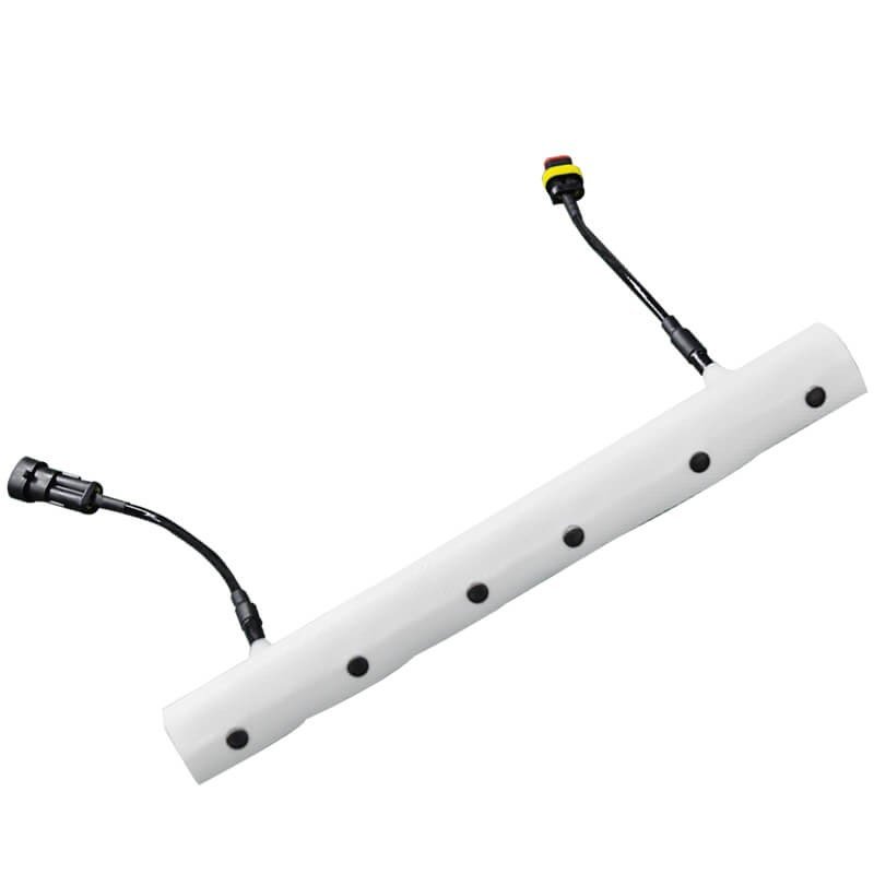
Multi-zone linear heating element with independent zone control. Designed for uniform thermal profiles along gas lines and sub-fab piping.
Request specs →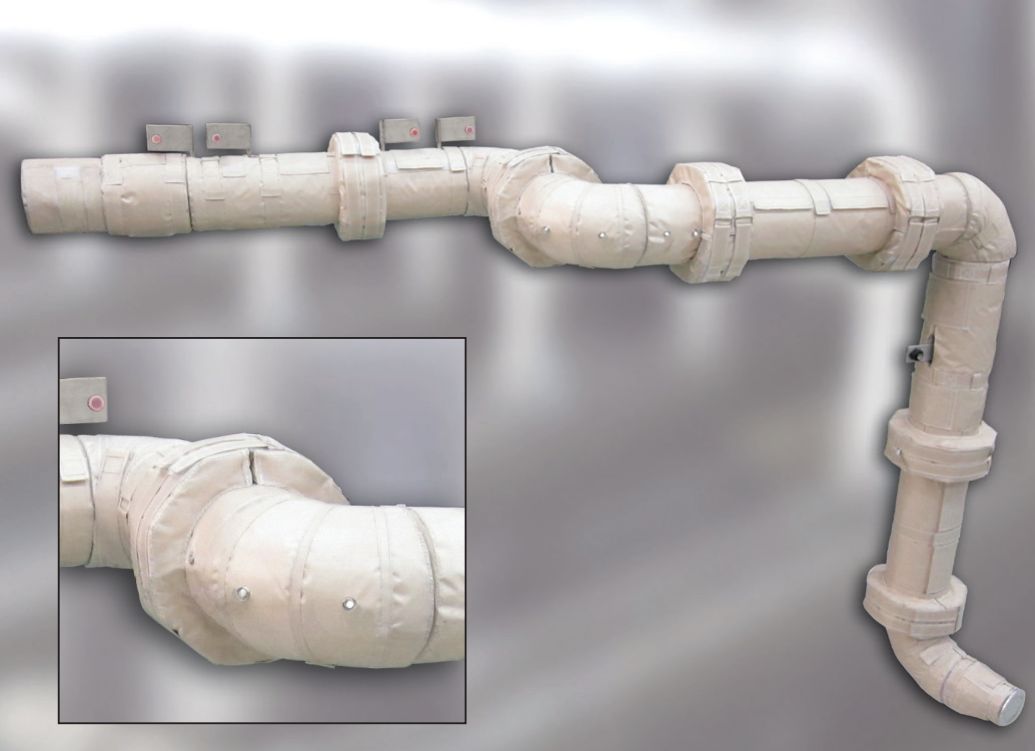
Custom-fitted flexible heater jackets for chamber bodies, valve manifolds, and irregular geometries. Integrated thermal control for precise temperature regulation.
Request specs →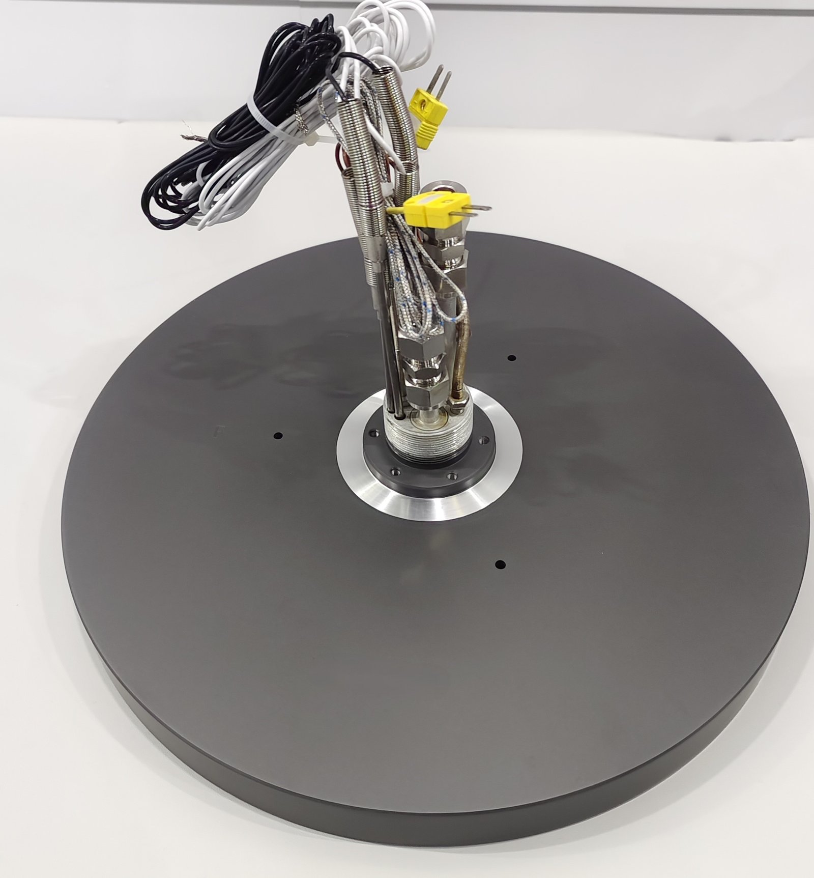
Large-diameter wafer pedestal heaters with integrated thermocouple arrays. ±1°C temperature uniformity for CVD deposition and anneal processes.
Request specs →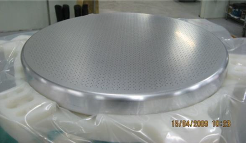
15-inch precision-perforated showerhead for CVD and ALD chambers. Thousands of holes machined to tight positional and diameter tolerances for uniform precursor distribution.
Request specs →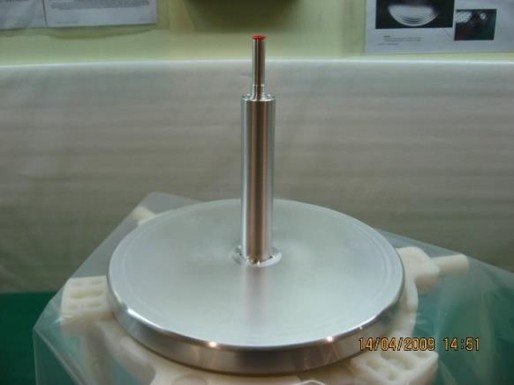
13-inch showerhead with integrated center stem for dual-channel gas delivery. Machined from high-purity aluminum or stainless steel to OEM specifications.
Request specs →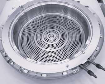
High-density multi-zone showerhead for advanced process chambers. Independently fed zones for radial gas distribution control in leading-edge deposition tools.
Request specs →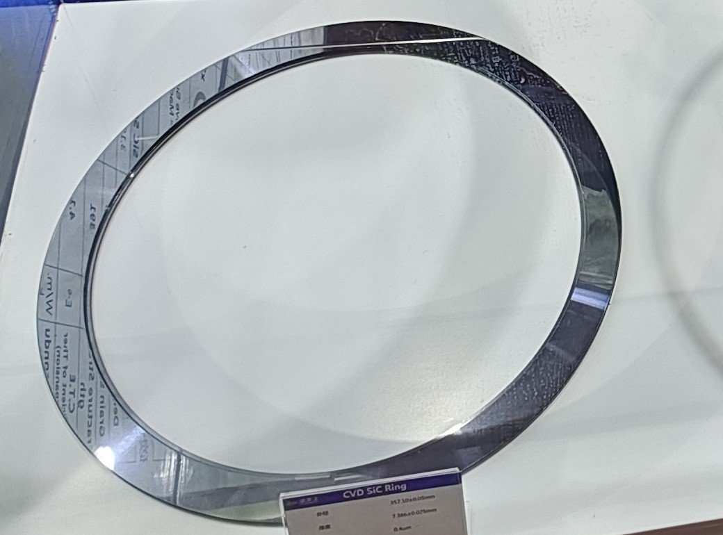
Chemical vapor deposition silicon carbide rings for etch and CVD chambers. Exceptional plasma resistance and thermal stability. Tight ±0.05 mm dimensional tolerance.
Request specs →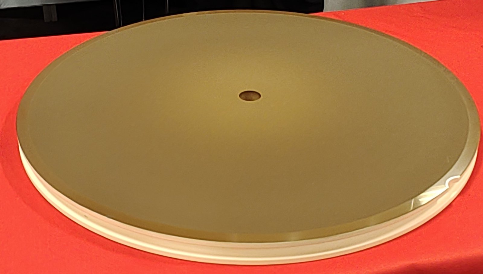
Transformer-coupled plasma (TCP) windows with specialized ceramic coating. Optimized dielectric properties and plasma erosion resistance for ICP etch tools.
Request specs →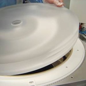
Complete TCP window replacement assemblies including matched O-rings for reliable vacuum chamber sealing. Ready-to-install PM kits for faster tool turnaround.
Request specs →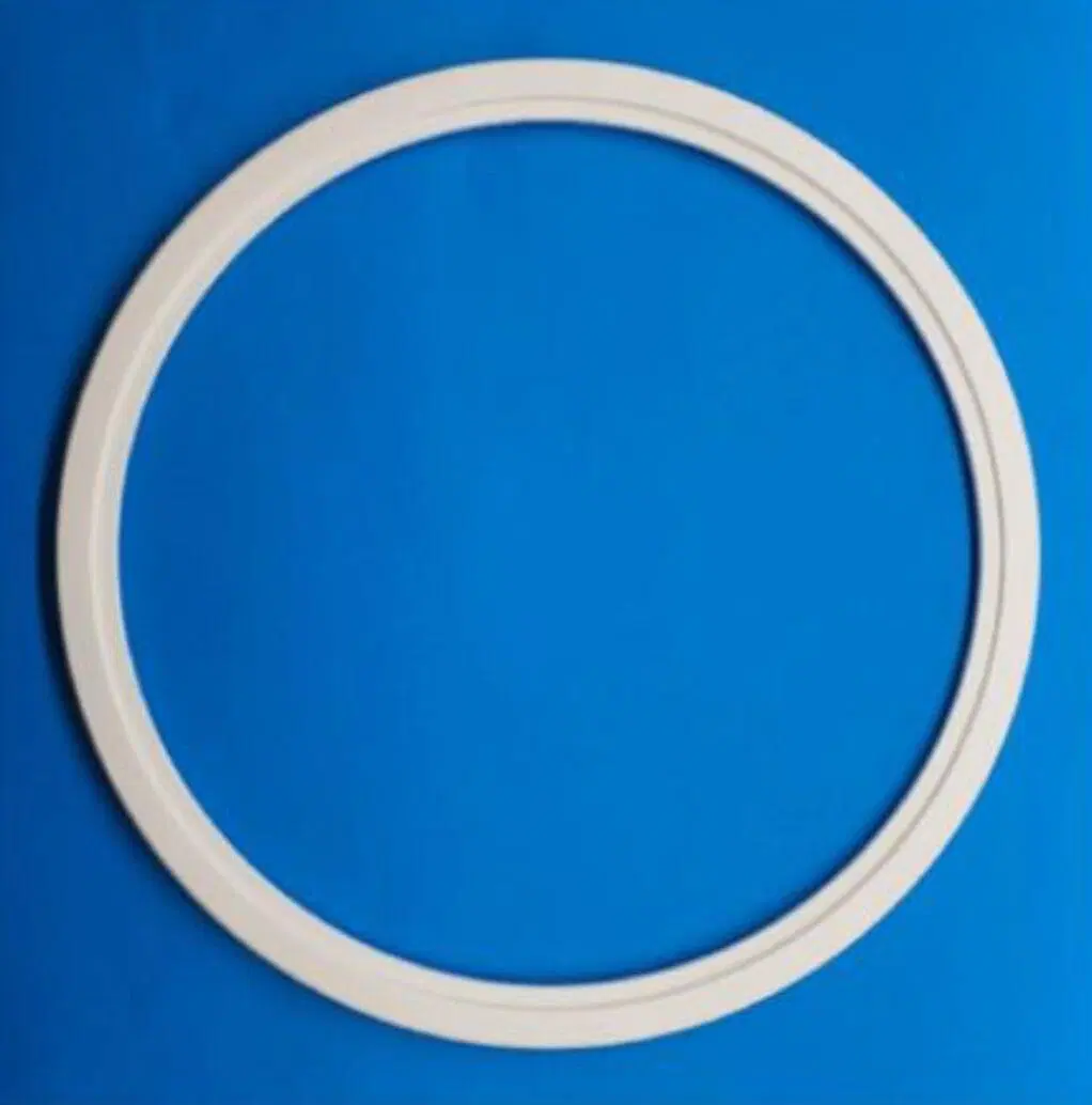
Precision-machined focus rings for semiconductor etch equipment. Compatible with leading OEM platforms. Available in quartz, silicon, SiC, and alumina grades.
Request specs →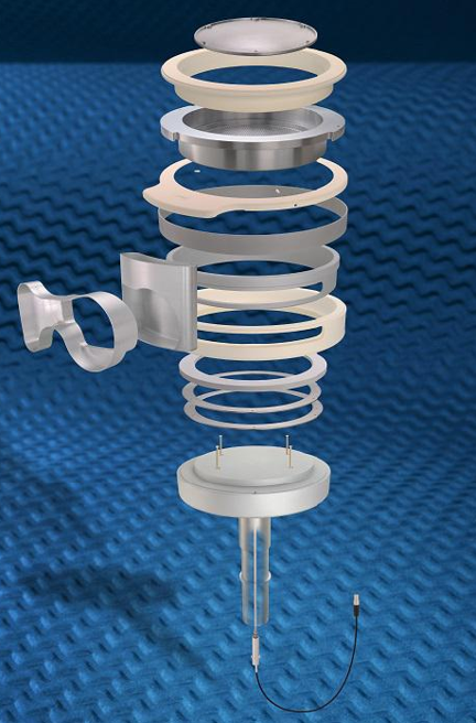
Complete chamber PM kits including rings, faceplates, and sealing components. Reverse-engineered to OEM form and fit for rapid preventive maintenance turnaround.
Request specs →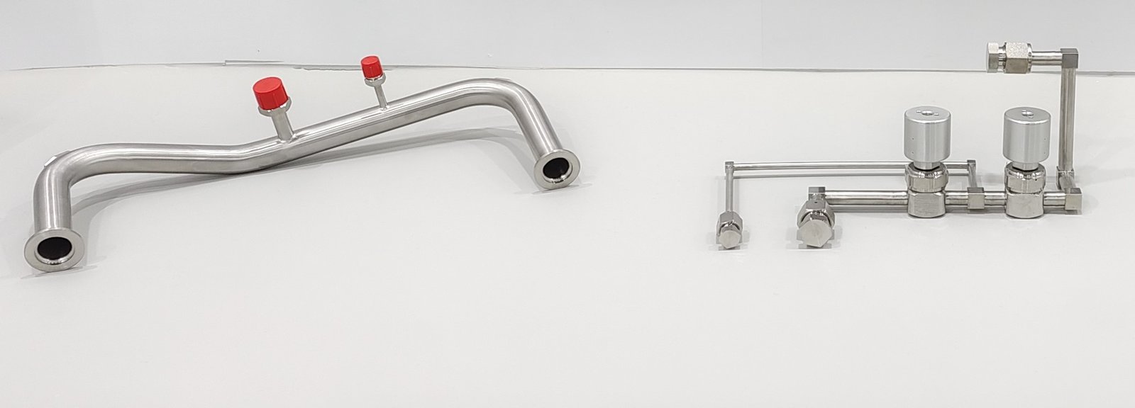
High-purity electropolished stainless steel gas line and weldment assemblies. Orbital-welded joints, helium leak-tested to 1×10&sup9; scc/s for ultra-high-purity gas delivery.
Request specs →
Refurbished and new-build electrostatic chuck assemblies for etch and deposition platforms. Full electrical performance testing and dielectric verification included.
Request specs →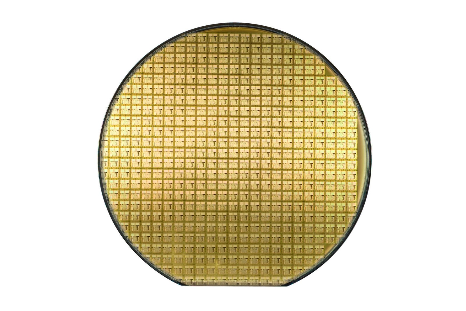
Custom coated and metallized wafers and substrates for calibration, process development, and specialized applications. Available in silicon, sapphire, and compound semiconductor materials.
Request specs →In-house precision machining, metrology, surface treatment, and system integration for semiconductor equipment components.
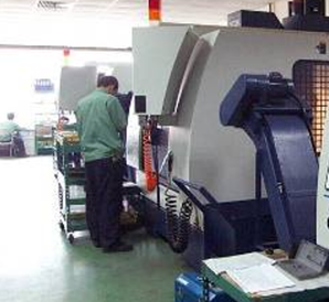
Multi-axis CNC machining of complex semiconductor components in aluminum, stainless steel, titanium, and specialty materials to ±0.001″ tolerances.
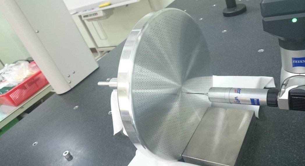
Full CMM dimensional inspection and 3D scanning using Zeiss and Hexagon systems. Certified inspection reports to SEMI standards with micron-level accuracy.
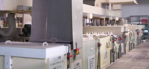
Hard anodizing, electroless nickel plating, ceramic spray coating, and specialty surface treatments. Qualified for semiconductor process-critical components.
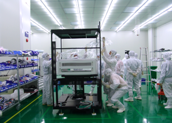
Clean-room-ready assembly and integration of process equipment sub-systems. Full functional testing, leak checking, and commissioning support before delivery.
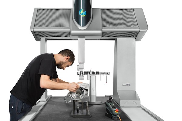
Precision measurement and reverse engineering of legacy or obsolete semiconductor parts. From physical measurement to full 3D CAD reconstruction, ready for production.
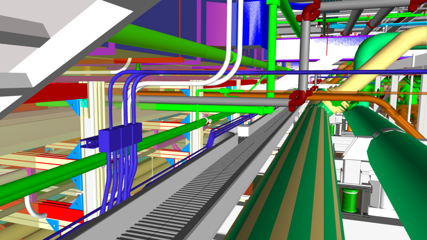
Building Information Modeling (BIM) for sub-fab utility, gas, and exhaust systems. Clash detection, installation planning, and as-built documentation for new and retrofit fabs.
FabProcisions delivered exceptional engineering solutions, showcasing expertise in semiconductor equipment manufacturing and assembly.
FabProcisions provided outstanding reverse engineering services for our critical equipment components. Their metrology expertise and attention to detail exceeded our expectations. Turnaround was faster than any other vendor we've worked with.
The field engineering team from FabProcisions handled our fab hookup with professionalism and precision. Their orbital welding and onsite support were instrumental in getting our new equipment operational on schedule.
We've been working with FabProcisions on custom heater jackets and ceramic parts for over two years. Their quality is consistently excellent and their pricing is competitive. A reliable partner for our semiconductor manufacturing needs.